Schematic Driven Cell Layout Using ADK
1.
Draw the schematic of a CMOS NOR gate
In
this lab, you will use both DAIC and ICStation in cooperation to design a
CMOS NOR gate.
1.1 Move into the directory you created for this class, create a directory for lab 5, and move into it. Then start DAIC:
>> cd egre533
>> mkdir lab5
>> cd lab5
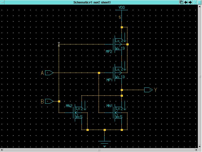
>> adk_daic &1.2 Open a sheet called nor2. Use your knowledge of Design Architect to create a schematic of a CMOS NOR gate like the one below. Note the pmos transistors have width=13.
1.3 Check and save your nor2 schematic by left clicking on the Check and Save button in the edit schematic palette. Fix any errors.
2.
Simulate your design using ELDO.
2.1
Simulate your schematic as you did in lab1 to make sure it functions as a nor
gate. Click the Simulation button in the edit schematic
palette. Select the Environment option under the Session
button, make the dialogue box look as shown then left click OK.

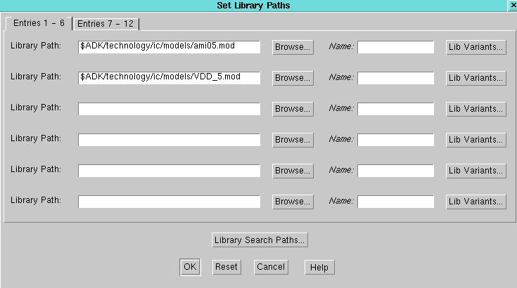
2.2 Set the libraries for simulation as you did in lab1by left clicking the Lib/Temp/Inc button, choosing Libraries, specifying the ami05 and VDD models (make the dialogue box look as below) then clicking OK.
2.3 Next left click the Analyses button, check only the box beside Transient, left click the Setup button beside Transient, set the start at time = 0 nanoseconds, run the simulation for 100 nanoseconds, then click OK in the setup transient analysis box and OK in the Analyses box.
2.4 Select A by left clicking on it (the net should turn white). Then left click the Forces button and choose Add. Make the resulting dialogue box look as shown to generate a 100 ns square wave.

2.5 Repeat the above procedure to force a 50 nanosecond square wave for B.
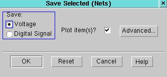
2.6 Setup the outputs from the simulation. You want to probe signal A, signal B and signal Y. You want each signal plotted as a separate line on the diagram so set them up one at a time. First select A. Then left click on the Probes/Plots button and choose Save Selected. Make the resulting dialogue box look as shown then click OK. Repeat for signals B and Y.
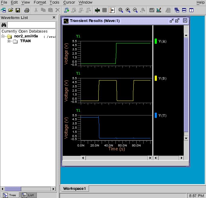
2.7 Run the simulation by left clicking the Run ELDO button. As before you will see three windows open. The first is a transcript window from the Netlister; if there are no errors then it should close automatically (see your Setup->Environment). The second is a transcript window from the ELDO simulator; it also should close automatically when the simulation is successful. The third is the EZwave waveform viewer. Make sure your waveforms are similar to the ones below then close the EZwave viewer. (As before, if you have any errors select the View Log option under the ASCII Files button in the Results section of the palette to view the log of your simulation.) Fix any errors and simulate until your nor2 schematic is correct.
2.8 Left click on the End Sim button in the palette to complete simulation and return to schematic edit.
3.
Add a symbol and create an LVS file
You
need a symbol for your nor2 gate for two reasons, (1) to establish connectivity
by defining input and output pins and (2) to enable you to use your nor2 gate
in more complex designs. In lab1 you created a box type symbol for your
inverter. Here you will create a symbol that looks like a nor gate.
Remember the problem with running the simulator! You must now close DAIC then start it again as you did in lab1 (else DAIC will not be able to properly add a symbol to your design).
3.1 Close DAIC. Make the Unix command window active and press Return. Then start DAIC as you did before (type in adk_daic & followed by Return). Then use the Schematic button in the right hand palette to open your nor2 schematic for editing.
3.2 Select Miscellaneous->Generate Symbol from the top menu bar. Then in the Generate Symbol dialogue box left click on the Choose Shape button. Make the resulting dialogue box look as shown then click OK. Click OK again the Generate Symbol dialogue box.

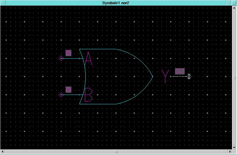
3.3 DAIC will open a new window containingf your symbol for you to edit. You will need only to add a "bubble" just before the output pin. BE SURE TO MOVE THE PIN, THE CONNECTING WIRE AND THE DIRECTION. Press the "-" key to zoom out. Select the entire pin assembly (all three components) by holding down the left mouse button and drawing a box containing the pin wire, the OUT box and the little diamond shape but not touching any of the body of the or gate. Then move the pin assembly right as shown below.
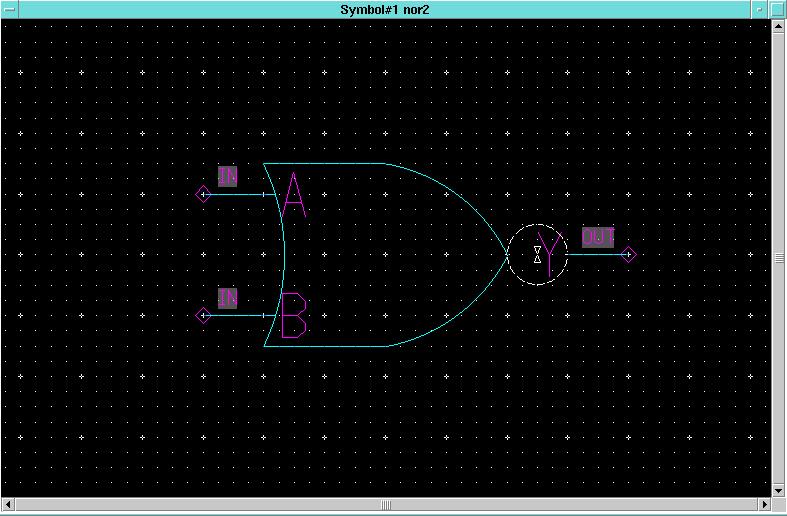
3.4 Now add a bubble to the output. Choose Circle under the Add portion of the palette. Put the cursor where you want the center of the circle (halfway between the end of the or gate and the beginning of the pin. Hold the left mouse button down and drag the cursor outward until the bubble is the right size as shown below.
3.5 Press F2 to unselect the bubble. Remember the quirk about symbols - first select File->Check Symbol then File->Save Symbol then File->Check Symbol again. After the second check you should have no warnings and no errors. Close the symbol editor window after you correct any errors.
3.6 Check the schematic by selecting File->Check Schematic from the top menu bar. You should have no warnings and no errors. Save the schematic sheet by selecting File->Save Sheet.
3.7 At this point you know that you have a proper schematic and a
proper symbol. There is only one more step required from DAIC - to
create the files necessary for layout. Left click on the Prep for
Layout button in the schemaitc edit palette. You will see a
transcript window for the Netlister. After it completes, close the
transcript window by pressing Return. Then exit DAIC.
4.
Use ICStation with schematic driven layout to start a layout of the CMOS NOR
gate.
Here
we are going to use one of the advanced features of ICStation within the Mentor environment
to have the schematic of the NOR gate help generate the layout. This function
is called SDL - Schematic Driven Layout. The layout functions within the Mentor
environment (along with the ADK design kit support) will help us to
automatically create the transistors via a device generator, and to
track the wiring of the cell so that it matches the schematic we originally
created. In the end, we can check the layout to see if in fact, it still
matches the schematic. This function is called LVS - Layout Vs. Schematic.
4.1 First you need to create some new viewpoints into the nor2 schematic. Viewpoints represent snapshots of your design taken with respect to different tools. You will need a LAYOUT viewpoint of your schematic which is created using the adk_dve script run from the command window. Make sure you are in the same directory as your nor2 design - lab5. Enter the command followed by the Return key as shown below. Note a lot of activity in the Unix command window as the script creates various viewpoints.
>> pwd
/students/YourName.../egre533/lab5
>> adk_dve nor2
After
the adk_dve script completes, start ICStation while still in your lab5
directory:
>> adk_ic &
4.2
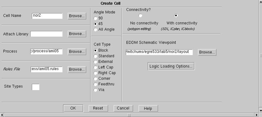
In the Session palette, under Cell, click on Create. In
the Create Cell dialog box that comes up, enter a cell name of nor2,
click the With connectivity button. Click the Browse...
button next to the EDDM Schematic Viewpoint box and select the layout
viewpoint under your nor2 component. Set the Process box to point
to the $ADK/technology/ic/process/ami05 process file and the Rules
File box to point to the $ADK/technology/ic/process/ami05.rules file
as you did for the full custom design. The result should be a dialog box like
the one below. Click OK.
4.3 Select the Context->Set Cell Config->Connectivity Editing menu item to put ICStation into the connectivity editing mode. This is VERY important when using SDL as it causes ICStation to warn you when an edit operation (such as adding a path) you are making on the current cell will merge 2 nets in the cell. Merging nets in the cell that should not be connected will cause the database to be corrupted such that extraction and LVS will no longer work correctly. Then remember to use Other->Window->Set Grid to set the SnapX and SnapY to 0.5.
4.4 Select Setup->SDL... from the top menu bar to setup SDL for this cell. You should see a dialogue box as shown below.
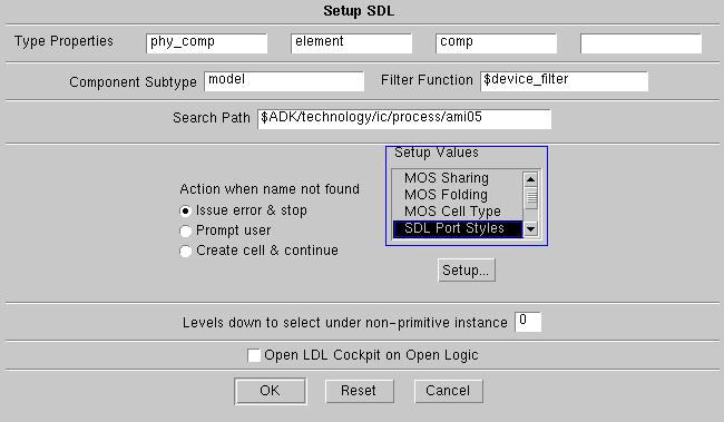
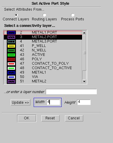
4.5 Select SDL Port Styles in the Setup Values listbox. Left click on the Setup... button. Choose Connect Layers, highlight METAL2.PORT, set Width to 4 and Height to 4 as shown below. Click OK for the Set Active Port Style dialogue box and OK for the Setup SDL dialogue box.
4.6 In the IC Palettes palette, click on DLA Layout (or ADK_Edit). In the DLA Layout (or ADK_EDIT) palette, click Logic->Open. The schematic of your nor2 gate should appear as below. Notice there are two windows. The window named IC 0: nor2 > nor2(i) is the IC layout window while the window named /:Sheet1: students/your_name/egre533/nor2/layout is the schematic window.

4.7 Create the power (VDD) and ground (GND) rails for the nor2 cell
by making the IC window active, placing the cursor in the IC window and
typing pr(). You should see the rails appear with N_Well
and P_Well above and below them in the proper spot. Note that the pr()
command is just a macro that has been provided for you to make layout easier.
This macro places METAL1 and METAL1.PORT in the proper places for
VDD and GND, makes them ports with those names, and places the N_Well
and P_Well. You can move or resize the resulting structures to match any
cell width or height you desire. If you do not use this macro, it is helpful to
at least create the VDD and GND rails and make them ports before proceeding
onto the next step so that the proper transistor connections to them are shown
when the devices are created.
5.
Place the transistors for the nor2 gate
Schematic
driven layout has two major advantages, first, as we will see, it keeps track
of the wiring of the cell and helps you make sure that it matches the
schematic. Second, it allows us to use the automatic device generators built
into ICStation to generate the transistors with the proper sizing as
specified in the schematic.
There are two ways to have the devices from your schematic generated and placed on the layout. The first way is to simply click on the AutoInst button under the DLA Layout palette. This will place all of the transistors in the schematic in the device for you and will merge devices together that can share common diffusion areas. This method of placing the transistors is often the fastest way to do it. The second way. should you wish to pursue it, is to manually place each transistor then manually combine them by manually flipping them so that shared diffusions are ajacent then using D Edit (the device editor) to join them.
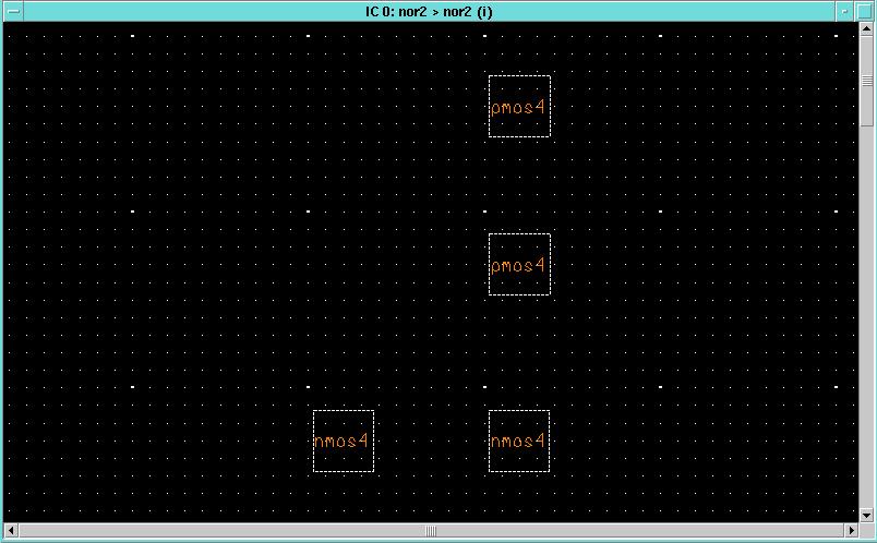
5.1 Make the IC layout window active then left click on the AutoInst button in the DLA Layout palette. You will probably see something similar to the screen shot below. This is another quirk of the tools and is easily fixed. These small boxes are just placeholders. Note there are four of them - one for each transistor in your design. All you need to do is delete all four of them then run the AutoInst again.
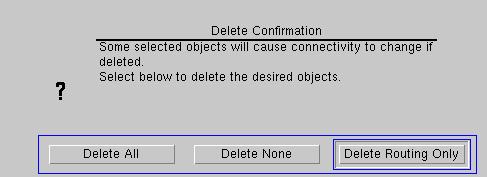
5.2 To delete the little placeholders, make sure nothing else is selected in the IC window by pressing the F2 key. Then select the placeholders by holding down the left mouse button and drawing a box around them (they will all turn bright white). Then press the Del key. Since you are deleting from the IC layout, IC Station will warn you that the connectivity may change by opening a dialogue box like the one below. Click the Delete All button.
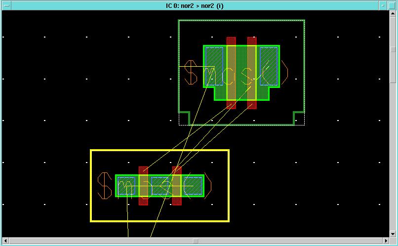
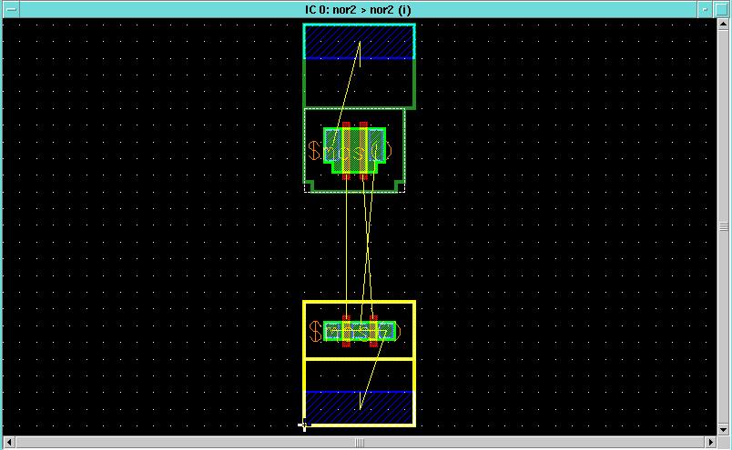
5.3 Left click on the AutoInst button again. This time the automatic instantiation should work and your IC layout window should appear as below. Note IC Station has combined the two PMOS transistors into a single PMOS structure by combing the drain of MP2 with the source of MP1 and combined the two NMOS transistors into a single NMOS structure by combining the source of MN1 and the source of MN2. This is diffusion sharing and makes your resulting IC layout smaller and simpler. Note also that IC Station has added several thin yellow lines. These lines are called overflows. Each one represents a connection that needs to be made (using POLY or METAL) in your layout. As you complete connections in the layout you will see the yellow overflows disappear.
5.4 Zoom out to show everything in the layout by either selecting View->All from the top menu bar or simultaneously pressing the Shift and F8 keys. Note IC Station has put the transistors above the power rails. You will need to move them to the appropriate positions - the NMOS structure (yellow) shoud attach to the P-Well above ground while the PMOS structure (green) should attach to the N-Well below VDD. You will also need to stretch the METAL1, METAL1.PORT, N_WELL and P_WELL as shown. Since the NMOS structure is slightly wider than the PMOS structure, your N-Well and VDD METAL1 and METAL1.PORT will stretch beyond the PMOS structure (keep your cells rectangular so they will be easier to combine)..
6.
Place the ports for the A and B inputs and the Y output
6.1
Make the schematic window active and select the B port. Make the IC
layout window active and click the Port button in the DLA Layout
palette. Place the resulting port at location 2,50. Do the same for
the A port and place it at 15,50. Finally, place the Y port at
28,50. Notice that the overflows now connect the ports with the proper
connections on the devices. When you have placed all three ports your
layout should look like:

6.2 Now that all the ports are in the layout, select Object->Add->Add Text to Port from the top menu bar then click OK in the dialogue box to add the text names to the ports.
6.3 Remember METAL2.PORT is only connectivity information. After you have placed the three ports, you must go back and add METAL2 with Aspect=Both to cover each port. As you add each 4x4 square of METAL2, you must make that a part of the port as well - else the Autorouter will not be able to locate your connections. Select Top from the DLA Layout palette then select Easy Edit from the IC Palettes palette. To add the METAL2 to a port:
a) Make sure nothing is selected {press F2}
b) Select a port {left click on the rightmost (output) port}
c) Add a METAL2 shape, 4 x 4, Aspect=BOTH covering the port {add shape METAL2,BOTH}
d) Terminate shape adding {press Esc}
e) Add the METAL2 to the port {select from the top menu bar Connectivity->Port->Add to Port while both the METAL2.PORT and METAL2 are selected}
Repeat
for the other two ports...
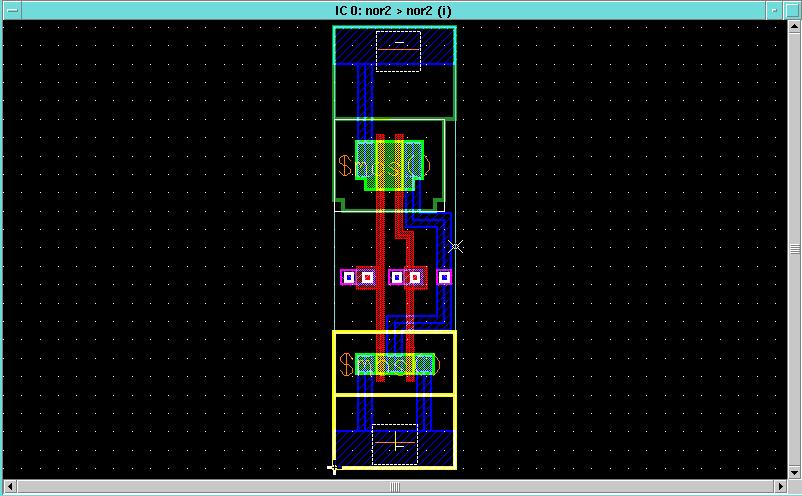
6.4 Use Add Shape and Add Path to add POLY and METAL1 to your layout. Don't forget you need CONTACT TO POLY to connect between METAL1 and POLY and you need VIA to connect between METAL2 and METAL1. Periodically check your design and fix any DRC (Design Rule Check) errors. Remember the nwc() and pwc() macros for adding N-Well and P-Well contacts. Your completed route will probably look something like the one below. You will use this layout in a larger design so add fp1 and METAL1.BLKG layers with Aspect=Both over the entire cell. Notice there is an overflow still on the screen even though GND is completely routed (the overflow between the P-Well contact and GND). This sometimes happens. Make sure your completed layout passes DRC (Design Rule Check) before proceeding.
7.
Check the correspondence of your cell to the schematic used to create it
Here
you will use LVS (layout vs. schematic) to be sure that your cell is wired the
same as your schematic.
7.1 First save the cell (from the top menu bar select File->Cell->Save Cell). Then close the schematic copy (from the DLA Layout menu select Logic->Close).
7.2 Go back to the IC Palettes palette and click on ICtrace
(M). In the ICtrace (M) menu, click on LVS. You will get an LVS
(Mask) dialog box. Under the Source Name box, click the Browse...
button then double click on the nor2 component ![]() and select the lvs design viewpoint
and select the lvs design viewpoint ![]() then click OK. Next set the Source Type
to eddm. Set Write Database to No.
So far your dialogue box should look like:
then click OK. Next set the Source Type
to eddm. Set Write Database to No.
So far your dialogue box should look like:

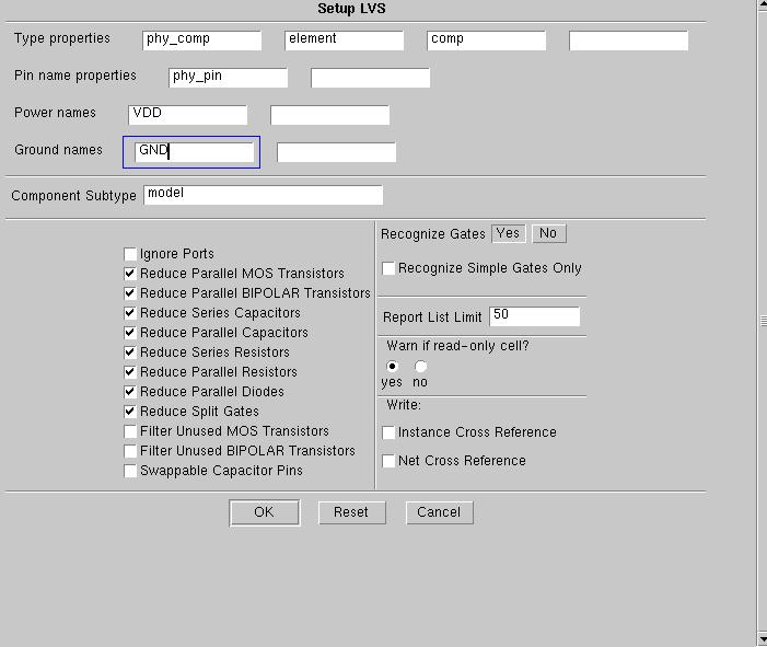
7.3 Now press the Setup LVS button. You will see a new dialogue box. Change the Ground names to GND as shown then click OK.
7.4 Now click OK in the LVS (Mask) dialogue box to run the LVS check. A number of messages will flash by at the bottom of the ICStation window with "Check completed..." as the last one.

7.5 To view the LVS results, select the Report item from the ICtrace (M) palette and select the LVS item from the popup menu that appears. The result should be a report window with the "smiley face" as shown below. If not, fix any problems and repeat the LVS. (Since you saved the cell it is no longer in edit mode. Use File->Cell->Reserve from the top menu bar to reserve the cell for edit if you need to make changes.)

8.
Extract the Spice netlist for the nor2 gate using Calibre PEX
The
thrid and final check you can perform on your layout before fabrication is a
Spice simulation of the actual layout - taking into account the various
parasitic capacitances and resistances of the process (AMI05 for this
example). This simulation will give you a good idea about the timing of
your circuit - how fast can you clock it, are there any timing hazards, etc
Extract the netlist using PEX as you did for the inverter in lab 3.
9.
Simulate the nor2 gate with ADiT
Simulate the nor2.sp file with ADiT as you did for the inverter in lab 3.
