1.1 Move into the directory you created for this class, create
a directory for lab 4, and move into it. Then start IC Station:
>> cd egre533
>> mkdir lab4
>> cd lab4
>> adk_ic &
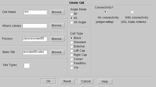
1.2 In the session palette window, click on CREATE with LMB (left
mouse button). Fill out the Create Cell dialog box like the one
shown below and click OK.

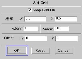
1.3 You may need a smaller grid for this and future tutorials.
Select Other->Window->Set Grid from the top menu bar, fill
out the resulting dialogue box as shown then click OK.

1.4 Create the power (VDD) and ground (GND) rails for the inv
cell by making the IC window active, placing the cursor inside the IC window
(where the dots are) and typing pwr() followed by the Return
key You should see the rails appear with N_Well and P_Well
above and below them in the proper spot. Note that the
pwr() command
is just a macro that has been provided for you to make layout easier. This
macro places METAL1 in the proper places for VDD and GND, covers
the METAL1 with METAL1.PORT, makes them ports with those
names, and places the N_Well and P_Well. You can move or
resize the resulting structures to match any cell width or height you desire.
ICStation has
a feature called device generators built into it that can layout a structure
automatically for you. Device generators are a lot like the pwr()
macro you used above except that they create a separate design unit, almost
like another cell, that gets instantiated into your layout. The ADK design
kit has device generators for NMOS and PMOS transistors which we will use
for this design.
2.1 Click on the DLA Device item in the IC Palettes palette
and click on AddMos in the DLA Device palette. Select the
pmos4
device and set the width to 10 (which means 10 lambda units)
and length to 2 (remember, length is always 2 lambda for
a standard CMOS transistor!). The sequence parameter tells the device
generator what combination of polysilicon gates and contacts you want in
the transistor. For this transistor, the default cgc, which means
contact-gate-contact
is what we want. For a diffusion shared string of three transistors the
sequence would be cgggc meaning
contact-gate-gate-gate-contact.
You can have any arbitrary sequence of gates and contacts and also specify
a different width for each transistor by putting a comma separated list
of numbers in the width field.
When you have the MOS Parameters dialog box setup like the one
below, click OK.

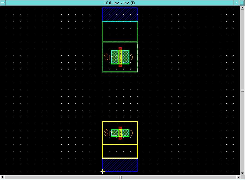
2.2 Click the LMB in the cell window near where you want the PMOS transistor
and when it appears, move it so that the upper left-hand corner of the
N_WELL
surrounding it lines up with the corner of the N_Well under the
VDD rail.
2.3 Click on AddMos again and select the nmos4 device
with a width of 5, a length of 2, and a sequence of cgc
in the MOS Parameters dialog box and click OK.
Place the resulting NMOS transistor next to the P_WELL above the GND rail.
The resulting layout should look like the one below.

Note that only part of the transistor layout within the MOS device is
shown at this level. There are N_PLUS_SELECT, P_PLUS_SELECT,and
CONTACT_TO_ACTIVE
shapes inside these devices that make them complete transistor layouts.
If you want to see what is inside a MOS device, select it (the $mos()
lable
will turn white when the entire device is selected) and use the
Context->Hierarchy->Peek
item from the pull down menu to bring up the Peek dialog box. Set
the Number of Levels item to 1 and click OK. You will
then see all of the layers in the MOS device. To go back to the external
view of the MOS device, select it and use the
Context->Hierarchy->Unpeek
menu item.
2.4 Use your skills in ICStation
to complete the layout so that it looks like the one below. Don't forget
to put METAL2.PORT with Aspect=Both over the METAL2
(also with Aspect=Both) input and output. Make the METAL2.PORT
input a port with the name in1 and the METAL2.PORT output
a port with the name
out1. Then use the Objects->Add->Add
Text on Ports item from the drop down menu to bind the port names to
the ports. Then add the METAL2 to the ports Connectivity->Port->Add
to Port as you did in lab2. The
pc() macro is handy
for adding poly contacts and the nwc() and pwc() macros are
handy for adding N_WELL and P_WELL contacts. Do a DRC check
on the cell, fix any errors that are listed and save the cell.

ICStation has
another feature called LVS (layout vs. schematic) that can check a layout
and compare it against a transistor level schematic. We will use this capability
to check your layout against the inverter schematic you created and simulated
in lab1.
3.1 Go back to the IC Palettes menu and click on ICtrace
(M). In the ICtrace (M) palette, click on LVS.
For the Source Name browse to the ...egre533/lab1/inv/lvs
LVS file you created in lab1. Leave the Source Type at eddm.
Set Write Database to No. Left click on thte
Setup LVS button.

3.2 In the Setup LVS dialogue box, change the Ground
names from VSS to GND as shown below.
Click OK. Click OK in the LVS (Mask) dialogue
box as well.

3.2 You will know the LVS check has completed by watching the
status lines in the lower left hand corner of the IC Station window.
The phrase "Check completed. Total CPU time: 0.02; Total REAL time:
0.093172." (see below) indicates the check has finished.

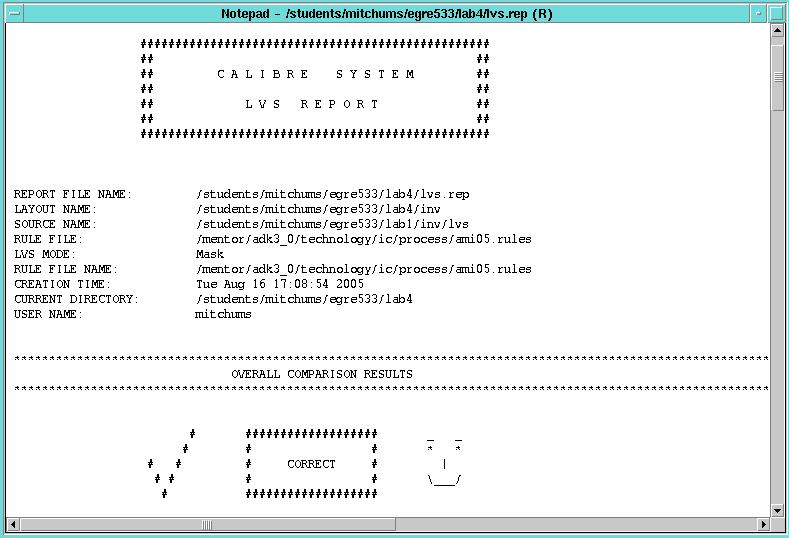
3.3 When IC Station has finished performing the LVS check
it will write the results to the Report Name file (lvs.rep).
You can view the results by left-clicking the small black arrow beside
the Report entry in the ICTrace(M) palette  then choosing LVS from the Report popup menu.
Your LVS report should look like below (Smiley Face) if you have a successful
comparison. You will probably have to scroll the report window down
to see the results (Smiley Face if successful or Frowning Face if there
are problems). The LVS report file is a regular ASCII text file so
you can use the Unix command cat to dump it to a console or terminal
window or you can open it with the text editor if you need to print it.

3.4 If your LVS does not match, fix any problems and run it again.
The LVS report will detail specific problems such as mismatched ports below
the Frowinng Face. Typical LVS problems are:
-
incorrectly defined ports in the layout or schematic
-
short circuits in the layout or schematic
-
missing shapes in the layout
3.5 Once you get LVS to match (so that you know your inverter as
built matches your schematic as designed), use Calibre PEX to extract
the parasitic spice netlist then simulate using ADiT as you did
in lab3.
3.6 Save the cell, close and exit IC Station.
