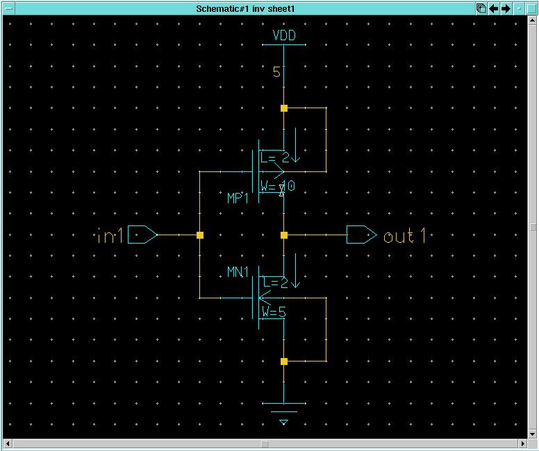
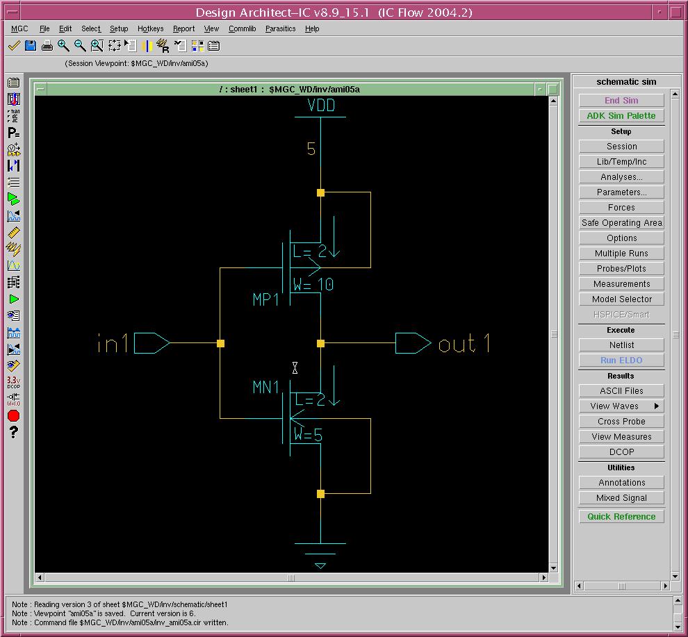
From the schematic edit palette left click once click on
Simulation to start the simulator. The border around your schematic
will turn green and you will see the simulation palette as shown below.
You will need to perform a little setup work for the simulator to operate
properly.

2.1 Setup the simluator itself by selecting the Session
button under Setup. You will need to setup three dialogue
boxes under this item. First choose the Simulator/Viewer option.
Make the resulting dialogue box look like the one shown below and click
OK.
Do not change the Advanced Options - they are set correctly by default.

2.2 Next select the Netlister option from the
Session button under Setup. Make it look as shown
then click OK. Be sure to enter GND beside
the Set Node 0 box - this informs the simulator thatGNDis
voltage ground (0 Volts).

2.3 Finally select the Environment option from the
Session
button under Setup. Make it look as shown then click OK.

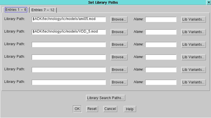
2.4 Setup the simulator to use the AMI05 process models by left
clicking the Lib/Temp/Inc button under Setup.
Then choose the Libraries option. Use the Browse button
to navigate to the ami05 model as shown. The ami05 model file is
located at /mentor/adk3_0/technology/ic/models. You must setup
the supply voltage because the ADK allows designs to be created for 2.5V,
3.3V and 5V logic. Your design in the ami05 process will use a 5
Volt supply. Specify VDD = +5V by setting the second Library Path
to the VDD_5 file as shown then click
OK.

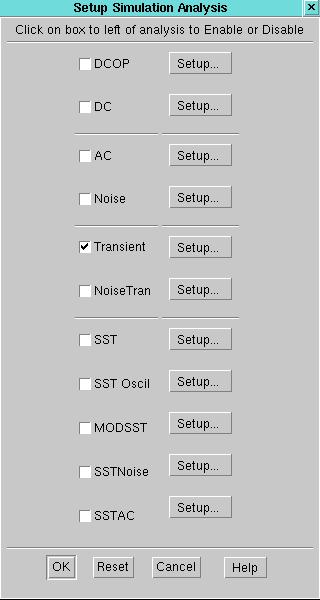
2.5 Setup a transient simulation. From the schematic
sim palette left click on Analyses under Setup.
In the Setup Simulation Analysis dialogue box check the box beside
Transient
as shown. Left click on the Setup button beside
Transient.
You will see the Setup Transient Analysis dialogue box. Fill
it out as shown then click OK. You have now setup a
simulation to perform transient analysis. The simulation will start
at time 0 nanoseconds and stop at time 100 nanoseconds. Click OK
in the Setup Simulation Analysis dialogue box also.


2.6 Define an input waveform for the inverter. First select
the
in1 signal on the schematic by left clicking on it. Then
select the Forces button on the schematic sim palette.
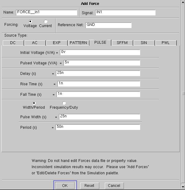
Choose Add from the list of choices. Then complete
the dialogue box as shown below. Note the waveform is defined using
the PULSE tab in the dialogue box. The other tabs (DC, AC,
...) represent other ways to define forces. Click OK.
This will create an input waveform to test your inverter. The input
will be a pulse which startss low (0v) at time 0 then pulses high (5v)
25 nanoseconds later and repeats at 50 nanosecond intervals. The
rise time and fall time of the pulse will be 1 nanosecond. Since
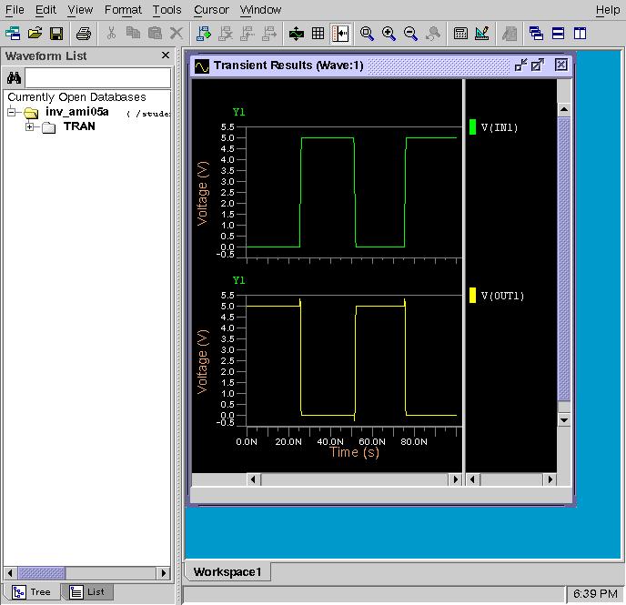
the stop time was set earlier at 100 nanoseconds, you should see two pulses.

2.7 Setup the voltages to be plotted by the simulation.
Select the in1 signal on the schematic by left-clicking on it.
Then left click on the Probes/Plots button under Setup
on the schematic sim palette. Choose Save Selected.
Fill in the dialogue box as shown below then click OK.
Repeat this procedure to add the out1 signal to the plot.

2.8 Finally, you need to scale the transistor values of L and W to the
correct value. For layout, these values are specified in Lambda units.
However, for simulation, they need to be expressed in microns. The easiest
way to do this is to put a scaling factor for Lamdba into the expression
for L and W on each transistor. If you do not do this, you will be simulating
the transistors with width and length values expressed in whole microns
and you will not get the correct results!
Place the cursor over the value of 2 for L on the PMOS transistor and
hit the <shift>< and F7> keys simultaneously. A dialog box like the
one below will open up:

Mover the cursor over the New Value item and change the value of 2 to
2*0.3 (Lambda for the AMI 0.5 process is 0.3 microns). Place the cursor
over the Type item and change it to expression. The dialog box will now
look like this:

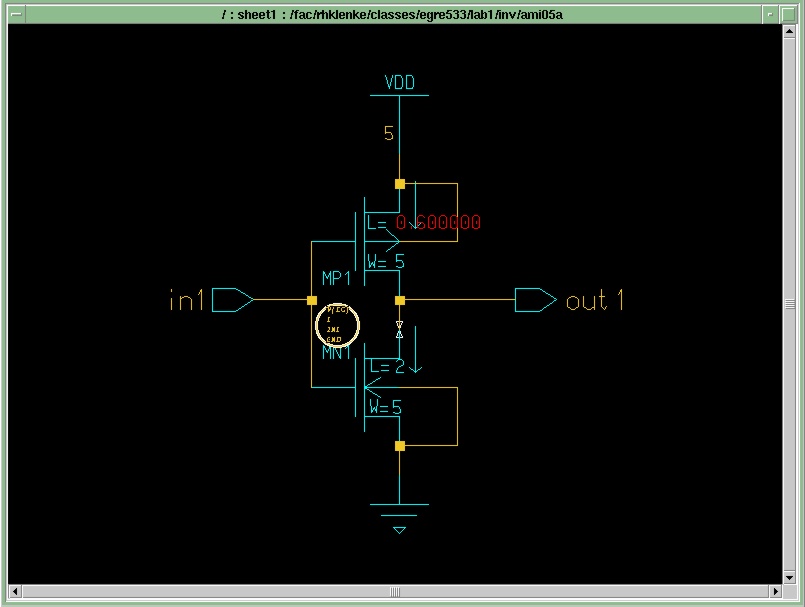
Hit the OK button on the dialog box. The new value for the L of the
PMOS transistor will be calculated and placed on the schematic. The resulting
schematic will look like the one below:

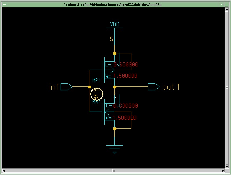
In a similar manner, change the values of the W parameter on the PMOS
to 5*0.3, and the L and W parameters on the NMOS to 2*0.3
and 5*0.3 respectively. The schematic will now look like the one
below:

You can now run the simulation and get the correct results for the devices
sized to the AMI 0.5 process.
Note that when you want to change the dimensions of the transistors
to balance them, you will do this by changing the value of
the multiplier in the expression for W, not by changing the value
of lambda. For example, to make the PMOS transistor twice as wide as it
is now, you would follow the procedure above and change the value of W
to 10*0.3.
2.9 Run the simulation by left clicking the Run ELDO
button under Execute on the schematic sim palette (ELDO is
the name of the simulator). You will see two text windows open, display
results then close as the simulation progresses. Your results should
appear as shown below. If you do not see the waveforms shown below
after a few seconds then left click on the ASCII Files button
under the Results section and choose View Log.
This will open a notepad window containing the log file for your simulation.
You can read the log file to locate your errors. When you have finished
reading the log file, close notepad by left clicking twice in the top right
corner of the window. Correct your errors and run the simulation
again.

2.10 Select File->Print from the EZwave window
to print your simulation results. Then close the EZ-wave viewer by
left clicking once in the top left corner of the EZ-wave window and selecting
Close.

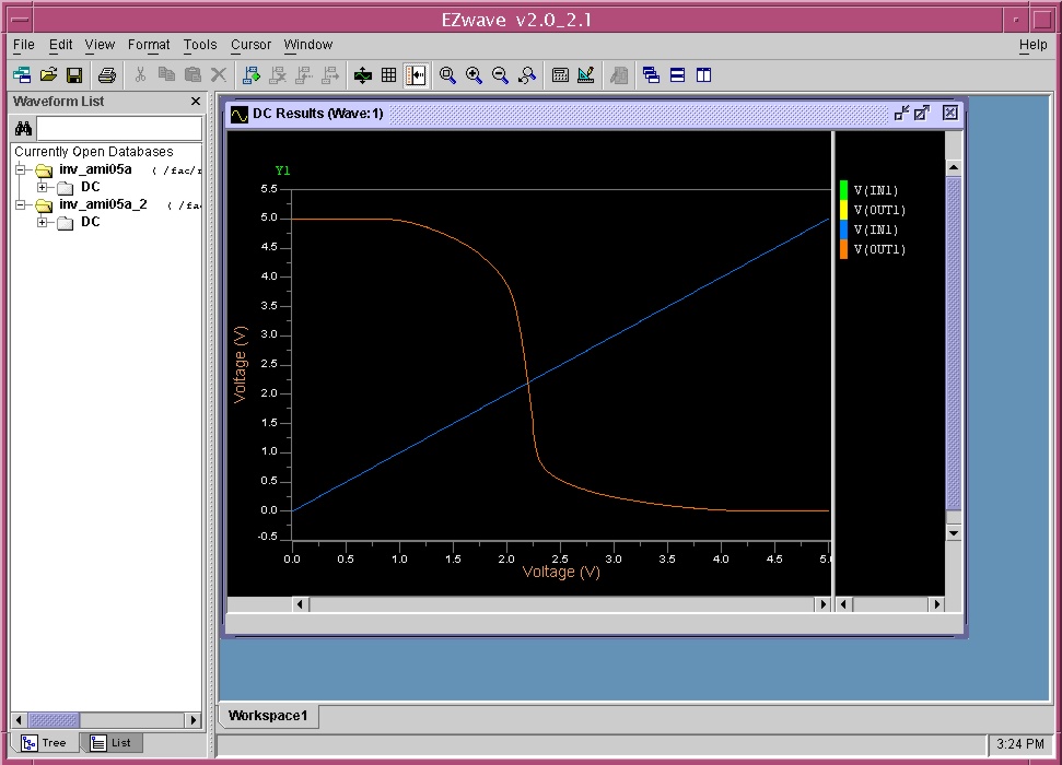
Now you will change the simulation to simulate the DC switching
characteristics of the inverter. You will program the simulator to
sweep the input voltage from 0V to 5V and plot the resulting output voltage.
This plot of VOUT vs. VIN will show the switching
threshold and noise margin for your design. You will need to delete
the FORCE and PROBES from the previous exercise and setup a DC analysis
instead of a transient analysis.
3.1 Delete the previous FORCE by left clicking on the Forces
button under Setup then choosing Edit/Delete/Show.
Select the force in the dialogue box by left clicking once on it then left
click on the Delete Selected button. The force should
be erased. Then left click on the Exit button.
3.2 Delete the previous PROBES by left clicking on the Probes/Plots
button under Setup then choosing Edit. Select
then delete each entry by first left clicking once on the entry to select
it then left clicking on the Delete button to delete it.
When you have deleted all probes from the previous exercise then left click
the OK button.
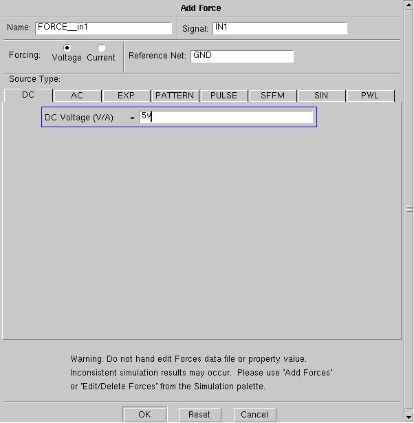
3.3 Add a DC force to the input signal (you will need a DC force
to sweep for voltage characteristics) by first selecting the in1
signal in the schematic window. Then left click on the Forces
button under Setup and choose Add. Use the DC
tab and make the dialogue box look as shown then left click OK.
You have defined a DC force necessary for the sweep.

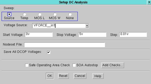
3.4 Left click on the Analyses button under Setup.
Uncheck Transient and check DC. Then
left click on the Setup button beside DC. Fill
out the Setup DC Analysis dialogue box as shown then left click
OK.
Left click OK in the Setup Simulation Analysis dialogue
box also.

3.5 Setup the signals to plot. This time you want both in1
and out1 plotted on the same chart (normal for viewing transfer characteristics).
First select in1 by left clicking on it in the schematic window.
Next hold down the control key on the keyboard and left click on the out1
signal. Both signals should now be selected (dashed). Now left
click on the Probes/Plots button under Setup and choose
Save
Selected. Mkake sure the resulting dialogue box looks as
before (Save Voltage selected, Plot Items checked)
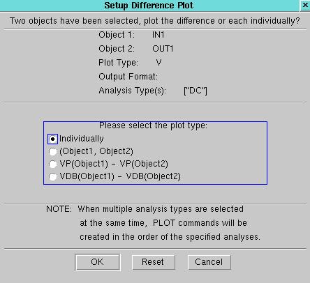
then left click on the OK button. This time, since
you have specifed more than one signal to plot, the simulator will bring
up an additional dialogue box. Fill it out as shown below then left
click OK.

3.6 Run the DC sweep by left clicking on the Run ELDO
button under Execute. As before, wait for the netlist window
then the simulation window to open and close. After a few seconds
the waveform window should open and you should see a plot similar to the
one below. As before, if you do not get the desired results then
left click on the ASCII Files button under Results
and choose View Log. Look through the log file to find
your errors and correct them.

3.7 Close the EZ wave window. Then select the End
Sim button under schematic sim to terminate simulation.
Then close your DAIC window.
Based on the tutorial prepared by David Zar.
